

Introduction to Silicon Photonics
Silicon photonics refers to the application of photonic systems for data transmission using silicon as an optical medium due to its exceptional advantages. This article will help you understand how silicon photonics works and its revolutionary impact on modern technology.
What is Silicon Photonics?
Silicon photonics is a cutting-edge technology that leverages silicon as an optical medium to transmit and process data using light. Unlike traditional electronic circuits, which rely on electrons for data transfer, silicon photonics utilizes photons to achieve high-speed communication, reduce power consumption, and increase bandwidth.
By integrating optical components with conventional semiconductor manufacturing processes, silicon photonics enables the operation of compact and high-performance photonic circuits that are scalable and cost-effective. This technology plays a crucial role in modern-day data communication, computing, and applications with sensing features.
Why Silicon?

Silicon has long been the foundation of the semiconductor industry, making it a natural choice for photonic applications. The adoption of silicon photonics is due to its availability, compatibility with existing fabrication technologies, and unique optical properties. As one of the most abundant elements, silicon is both cost-effective and sustainable. Silicon benefits from mass-scale production in the electronics industry, significantly reducing manufacturing costs, unlike expensive materials like indium phosphide or gallium arsenide.
Apart from cost efficiency, silicon is highly compatible with Complementary Metal-Oxide-Semiconductor (CMOS) technology. This compatibility allows photonic circuits to easily integrate with electronic components on a single chip while reducing power consumption and minimizing signal loss. Although silicon is not naturally efficient at emitting light, it excels in guiding and modulating optical signals.
Moreover, recent advances in hybrid-integration now let silicon photonic circuits be co-packaged with standard CMOS electronics, while still embedding active optical components—such as on-chip lasers and photodetectors—to overcome traditional limitations. Furthermore, scalability is a major advantage of silicon photonics. With ongoing advancements in nanofabrication, silicon photonic devices can be manufactured at the smallest scales without compromising performance.
Building Blocks of Silicon Photonics
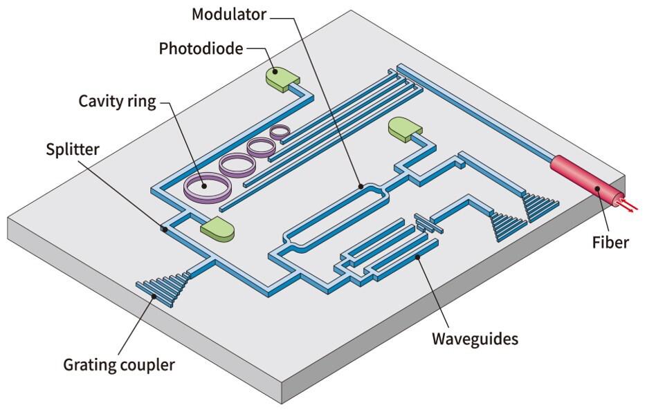
Understanding the building blocks of silicon photonics can help you have a thorough idea of its functionality.
Optical Waveguides
Optical waveguides form the foundation of silicon photonic circuits by directing and confining light signals. These structures, fabricated from silicon or silicon nitride, enable efficient signal transmission with minimal loss. Their design is crucial in determining overall system performance, with parameters such as waveguide width, height, and material composition affecting propagation loss.
Optical Resonators
Optical resonators, like ring resonators, enhance light interaction within silicon photonic devices, making them essential for filtering, modulation, and wavelength selection. By trapping light within a confined structure, these resonators improve efficiency and enable high-precision optical processing. Optical resonators are widely used in applications such as optical sensors, lasers, and multiplexing systems.
Electro-optic Modulators
Electro-optic modulators manipulate light properties (phase, intensity, polarization) for high-speed optical communications using materials like lithium niobate and PLZT. While silicon modulators exist through carrier effects, they typically underperform dedicated electro-optic materials in speed and insertion loss.
Photodetectors
Photodetectors convert optical signals to electrical ones for communications and sensing applications. InGaAs devices excel in infrared detection, while silicon photodetectors serve visible and near-infrared applications with monolithic integration capabilities. Sensitivity, response time, and noise characteristics determine system performance in data transmission and imaging applications.
Coupling Elements
Coupling elements facilitate efficient light transfer between different components in a silicon photonic system. Whether coupling light from an external fiber or between on-chip waveguides, these elements minimize optical loss and improve signal integrity. If we talk about commonly used techniques, grating couplers, and edge couplers have the most common application due to their unique advantages.
Key Applications
The versatile function of silicon photonics makes it a highly valuable technology for various industries across the globe. We have covered the most common applications below for your reference.
Data Centers

Silicon photonics is changing data center infrastructure by addressing the growing demand for higher bandwidth and energy efficiency. Traditional electrical interconnects face limitations in speed and power consumption, making optical solutions a necessity. By replacing electrical links with optical connections, silicon photonics enables data transmission rates exceeding 400 Gbps while significantly reducing energy requirements.
Sensing and Medical Diagnostics

The high precision and miniaturization capabilities of silicon photonics have made it invaluable in sensing applications, especially in medical diagnostics. Optical biosensors based on silicon photonic technology are capable of detecting minute biological markers for early disease diagnosis, offering rapid and highly sensitive results.
Automotive and LiDAR Systems

The modern world heavily relies on LiDAR technology. It has become essential for autonomous vehicles and advanced driver assistance systems (ADAS). Silicon photonics is revolutionizing LiDAR by enabling compact, solid-state designs that replace traditional bulky mechanical scanning systems. With integrated photonic circuits, LiDAR systems achieve higher resolution and improved reliability while maintaining cost efficiency.
Performance Testing
Characterizing Photonic Integrated Circuits (PICs) presents unique challenges, especially as the industry shifts toward Wafer-Level Characterization (WLC) to reduce development time and cost. Unlike traditional methods where chips were diced and tested individually, WLC enables characterization directly on the wafer, allowing only the best-performing devices to proceed to packaging and volume production.
However, WLC introduces several technical hurdles:
Coupling Light Effectively
PICs often exhibit high Insertion Loss (IL) due to factors such as waveguide imperfections, coupling inefficiencies, and design-related variations. In the past, this issue made it difficult to inject sufficient optical power for testing. Santec’s TSL Type-H tunable laser addresses this problem by delivering high optical power (>100 mW or 20 dBm), ensuring sufficient signal strength even when IL is significant. This enables effective light coupling into the PIC during wafer-level testing.
Measurement Repeatability
A critical aspect of WLC is maintaining high repeatability, especially in aligning the optical fiber to the coupling interface. Minor variations in fiber placement can significantly affect measurement results. While capacitive sensors are commonly used to measure the distance between the fiber and the wafer, they become ineffective near wafer edges, exactly where precision is often required for edge-located PICs.
Santec’s solution to this challenge is the SPA-110, which uses an Optical Frequency Domain Reflectometry (OFDR) technique. This approach accurately measures the fiber-to-wafer distance by analyzing back-reflection from the fiber tip and the wafer surface, ensuring consistent and repeatable coupling even at the edges of the wafer.
Polarization Dependency
With the miniaturization of PICs, the state of polarization (SOP) of the input light becomes crucial. Certain waveguides or components may not transmit light efficiently unless the SOP is properly aligned. A poor match can appear as high coupling loss, when in fact it's due to Polarization Dependent Loss (PDL).
Santec provides tools that automatically find the optimal SOP to maximize coupling efficiency. Once the best SOP is determined, full characterization is performed under this condition, ensuring accurate and reproducible measurements.
Detecting Fabrication Defects
In mass production, fabrication errors such as waveguide discontinuities or defective components can compromise circuit integrity.
Santec’s SPA-110 can detect abnormal back-reflection peaks, helping identify faults like broken waveguides or improperly processed elements. It allows manufacturers to screen and improve production yields.
Recommended Tools: Santec LIS Solutions
When it comes to silicon photonics testing, Santec is a name of trust and reliability. At Santec, you can find a range of advanced solutions designed to meet the demands of both research and production environments. Here are the most popular testing solutions you can get for efficient silicon photonic testing.
STS Swept Test System
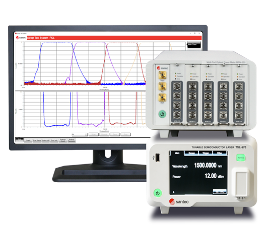
Santec’s STS (Swept Test System) is a comprehensive solution for photonic testing, offering high-speed analysis, high resolution, and superior accuracy. It integrates a tunable laser (TSL-775 or TSL-570), an optical power meter (MPM-220), a polarization control unit (PCU-110), and custom software to optimize WDL and PDL measurement.
TSL-570 Type H High Power Tunable Laser
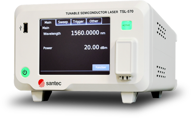
The TSL-570 Type H is a high-performance tunable laser, delivering peak optical output power over 20 dBm. With an optical cavity design, it offers picometer accuracy, sub-picometer resolution, and rapid scanning speeds of up to 200 nm/s. TSL-570 supports both O-band (1260-1360 nm) and CL-band (1500-1630 nm) tuning, making it a versatile tool for optical component characterization, photonic circuit testing, quantum photonics, spectroscopy, and sensor applications.
SPA-110 Swept Photonics Analyzer (Long Range Model)
The SPA-110 is an advanced optical frequency domain reflectometry (OFDR) analyzer that enhances Santec’s tunable lasers for detailed photonic component analysis. With a sampling resolution of 5 µm, it enables precise characterization of photonic integrated circuits (PICs) and silicon photonic (SiPh) devices. Compared to conventional OTDR technology, the SPA-110 offers significantly higher resolution and accuracy, making it ideal for analyzing compact and complex optical setups.
LLP-100 Laser Lock Pro
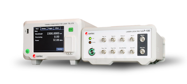
The LLP-100 Laser Lock Pro is a frequency control module designed to work with Santec’s TSL-570 laser system. It enables precise frequency locking by processing an electrical error signal derived from an external reference. Through dedicated PC software, users can simultaneously control the TSL-570 and LLP-100, ensuring stable and optimized frequency lock conditions.
The Takeaway
The above article can help you develop a thorough understanding of silicon photonics and its applications in the modern world. With active influences in industries like healthcare, automotive, and data centers, this super-efficient technology is making breakthroughs in optical computing. If you need efficient and reliable photonic testing equipment, explore the Santec website to find what you need.