

Introduction to Silicon Photonics
The shift toward higher data rates and lower latency places new demands on network infrastructure. Co-packaged optics (CPO) is emerging to respond to these demands, offering a way to integrate optical I/O directly with switch ASICs. This integration reduces power consumption, improves signal integrity, and allows for more compact designs.
CPO is gaining attention across high-performance computing, AI clusters, and hyperscale data centers, where traditional pluggable modules are beginning to reach their limits. As system complexity increases, so does the need for accurate, repeatable testing.
This blog outlines how co-packaged optics work, why they matter, and how companies like Santec support their development with precision testing tools.
What Are Co-Packaged Optics?

Co-packaged optics (CPO) refers to integrating optical transceivers and switching ASICs within a single package. Instead of connecting the switch chip to pluggable optical modules through electrical traces on a printed circuit board (PCB), CPO brings the optics directly adjacent to the chip. This shift significantly reduces the length and complexity of the electrical connections between them.
Traditional architectures separate the electrical and optical components. Signals must travel several inches across the board, encountering resistance, heat, and latency. Co-packaged optics reduce this distance to just millimeters. The result is lower power consumption, improved signal integrity, and higher throughput potential.
As data rates climb, the limitations of copper interconnects become more apparent. CPO addresses these issues by moving optics closer to the switch chip, minimizing losses, and increasing system efficiency.
Evolution from Pluggable Modules to CPO
Historically, data center switches and routers have relied on pluggable optical transceivers. These modules are inserted into the front panel of networking hardware, offering the benefit of swappability and ease of upgrade. However, this approach introduces electrical bottlenecks as data rates increase.
Pluggable optics work well at lower speeds, but as lane rates push beyond 100G, signal degradation through copper traces becomes a serious limitation. These traces are not just inefficient; they also consume valuable power and require complex equalization techniques to function.
CPO eliminates these problems by embedding optical engines directly within the switch package. The result is a shorter electrical path, reduced energy per bit, and tighter integration overall. With no need for front-panel optical modules, designers can free up space for additional silicon or cooling.
An illustration comparing the two architectures would show key differences:
●Pluggable Modules: Located on the switch front panel, connected to the ASIC via PCB traces several inches long. More susceptible to signal degradation and higher thermal output.
●Co-Packaged Optics: Optics mounted beside the ASIC inside the same enclosure, minimizing trace lengths and improving performance per watt.
Visually, this comparison highlights benefits in bandwidth scaling, thermal efficiency, and signal clarity.
Why it Matters
Power Efficiency

Data centers are power-intensive. With the rise of artificial intelligence, machine learning, and cloud computing, workloads have become larger and more frequent. According to recent estimates, global data center energy consumption accounts for about 1–2% of total electricity use. Electrical input/output (I/O) operations consume a large portion of this power.
Co-packaged optics significantly reduce the energy required for I/O. By shortening the distance electrical signals need to travel, power consumption drops. As I/O speeds rise, this power savings becomes more critical to achieving sustainable infrastructure.
Bandwidth Scaling

The shift to 800G and 1.6T interfaces is no longer theoretical. It is driven by the scale and speed demands of AI training clusters, high-performance computing (HPC), and hyperscale cloud environments. These use cases require fast, parallel communication with minimal overhead.
Copper-based interconnects cannot scale efficiently to these data rates. Signal integrity becomes harder to maintain, and energy consumption rises sharply. Optical I/O, embedded through co-packaged designs, allows systems to support higher bandwidth without the limitations of electrical channels.
Signal Integrity

At speeds of 112G per lane and beyond, electrical signals degrade significantly over longer PCB distances. This degradation introduces noise, increases bit error rates, and reduces system reliability. Advanced equalization and signal conditioning techniques can only go so far in compensating for these losses.
CPO avoids the problem entirely by using optical interconnects that maintain signal fidelity over short and long distances. Optical signals are immune to electromagnetic interference and can carry more data with less degradation, even as data rates continue to rise.
Form Factor Constraints
Data center switches are limited by the physical space available on the front panel. As network demands grow, so does the need for higher port counts. However, there’s only so much real estate to work with on traditional systems using pluggable modules.
CPO resolves this issue by removing the need for front-panel optics. Optical engines can be placed around the ASIC, increasing density without expanding the device footprint. This design allows engineers to pack more connectivity into the same physical space, meeting the demand for higher port densities without requiring larger systems.
How Co-Packaged Optics Actually Work
Photonic Integrated Circuits (PICs) in CPO
Photonic Integrated Circuits, or PICs, are the primary components that enable optical communication in co-packaged optics. These circuits integrate multiple optical functions into a single chip, such as lasers, modulators, waveguides, and photodetectors . This integration enables handling light-based data transmission and reception without requiring separate, discrete components.
The benefit of this level of integration is significant. Instead of managing multiple components connected through fiber or other coupling mechanisms, PICs provide a single signal generation, modulation, and detection platform. This reduces complexity and improves signal stability across high-speed links.
PICs used in co-packaged optics often support multi-channel configurations. Each channel operates independently but shares the same substrate. This allows for high-throughput communication while saving board space and simplifying alignment. With multiple lanes of optical I/O consolidated into a small footprint, system designers can scale up bandwidth without increasing hardware volume.
By bringing optics closer to the switching ASIC, PICs reduce latency and power consumption while maintaining high signal integrity. Their role in co-packaged optics is not limited to transport—they are also critical to modulation precision and noise control.
Silicon Photonics and Optical Interconnects
One of the key enablers of PIC deployment in co-packaged optics is silicon photonics. This technology leverages standard CMOS manufacturing processes to fabricate optical components directly on silicon wafers. The result is a production method that is cost-effective, repeatable, and compatible with the existing semiconductor ecosystem.
Silicon photonics allows the integration of modulators, waveguides, splitters, and photodetectors on the same die. These components form the optical interconnects that carry data in and out of the switch chip. Because they are built using CMOS-compatible materials and tools, they can be manufactured alongside traditional electronics, minimizing the gap between optical and electrical domains.
This compatibility is critical to co-packaged optics. By allowing the optical engines to sit next to the ASIC, designers can create compact, high-bandwidth communication links that bypass the limitations of copper traces. The signal path is shorter, cleaner, and more energy-efficient, with reduced interconnect distance.
As bandwidth demands increase, scaling with silicon becomes more practical than discrete optics. Silicon photonics provides a platform to expand optical I/O capacity without increasing complexity. It also supports denser layouts, helping systems reach 800G and 1.6T targets without rethinking the entire switch architecture.
Thermal Management Challenges and Solutions
Bringing optical engines closer to switch ASICs creates several thermal challenges. The switch chip itself consumes significant power and generates substantial heat. Adding optical components—particularly lasers—into the same enclosure raises the thermal load further. Without proper thermal management, device performance and reliability are at risk.
Passive cooling strategies are the first line of defense. These include heat sinks, thermally conductive packaging materials, and optimized airflow. However, in dense CPO configurations, passive cooling alone is often insufficient.
Active cooling becomes necessary in many cases. This may involve liquid cooling loops, thermoelectric coolers, or microchannel heat sinks. These systems move heat away from critical components more efficiently than air cooling and can be precisely targeted to specific thermal zones within the package.
Thermal-aware design during the test and validation phase is essential. Understanding how temperature affects laser stability, wavelength drift, and modulation efficiency allows engineers to fine-tune the system before it reaches production. Accurate modeling and testing ensure the optical engines and ASICs operate within safe thermal limits, even under continuous high-speed operation.
Co-packaged optics require a balance between performance, size, and thermal control. Without effective thermal strategies, the advantages of closer integration can be offset by performance degradation or component failure.
Testing and Validation in CPO
Importance of Accurate Testing in CPO Development
Co-packaged optics introduce a tightly integrated design where optical and electrical components are placed side by side within a shared enclosure. This integration offers performance advantages and changes how systems are validated during development. Testing becomes more complex and critical, mainly because of the lack of component-level flexibility once the package is assembled.
In traditional architectures, a faulty transceiver or optical module can be removed and replaced. With co-packaged optics, this is not the case. Once optical engines are embedded next to the switch ASIC, there is no straightforward way to isolate or swap out individual parts. As a result, testing must be completed before final assembly. Any design or manufacturing errors caught late in the process can lead to the loss of an entire module.
Another consideration is performance tolerance. Photonic Integrated Circuits (PICs) and their optical components often operate within very narrow margins. Parameters like insertion loss, return loss, and extinction ratio must stay within specific sub-dB levels to meet design targets. Small deviations can result in degraded signal quality or failed compliance testing.
The cost of failure in this context is also higher. At the wafer or module level, rework is limited and usually impractical. A failed part doesn’t just delay development—it often means scrapping expensive hardware. For these reasons, accurate and repeatable testing at various stages, including wafer-level and module-level, is essential for validating performance and ensuring reliability.
Common Testing Challenges and Mitigation Strategies
Testing co-packaged optics presents several technical challenges, especially as the systems become more compact and channel counts increase.
Polarization Sensitivity
Many PICs exhibit polarization-dependent behavior due to their asymmetric waveguide structures. As light enters the device, the insertion loss can vary depending on the signal’s polarization state. This variation affects link performance and can introduce inconsistencies across channels. Testing systems must account for this by measuring polarization-dependent loss (PDL) and polarization mode dispersion (PMD) under controlled and repeatable conditions. Instruments capable of tracking these changes in real time help engineers fine-tune the optical design.
Wavelength Drift
Temperature fluctuations can cause wavelength drift in lasers and other optical components. This shift may misalign the modulator and detector operating points, especially in tightly spaced wavelength channels. Test equipment should measure wavelength stability and performance across expected operating temperatures. Environmental testing during development helps identify components or configurations prone to instability.
Crosstalk
High-density optical integration increases the likelihood of optical and electrical crosstalk between channels. This interference can reduce signal clarity and limit system bandwidth. Testing must include analysis of channel isolation and measuring near-end and far-end crosstalk. Optical Frequency Domain Reflectometry (OFDR) and other high-resolution tools can help detect sources of interference before they impact system operation.
Test Automation and Resolution
Manual testing is inefficient, given the number of parameters that must be validated across many ports. Automated systems improve throughput and consistency, especially in production environments. Instruments with high wavelength resolution, precise power measurement, and robust software interfaces allow for comprehensive, repeatable characterization of each optical path.
Developers can ensure that co-packaged optics meet performance targets and manufacturing standards by addressing these challenges with purpose-built testing tools. Testing is built into every stage of the development process.
Santec’s Solutions for CPO Testing
Overview of Santec’s Role in the CPO Ecosystem
Co-packaged optics require a testing infrastructure that can match their precision and complexity. Unlike traditional pluggable optics, where components can be tested in isolation, CPO demands system-level validation with minimal room for post-assembly correction. Santec provides the tools necessary to meet these demands.
Santec supports the CPO ecosystem with test and measurement instruments for optical component characterization, wafer-level diagnostics, and module-level validation. These systems are built to handle high-speed, high-density designs with requirements for sub-picometer resolution, polarization sensitivity, and repeatability across production lines.
By offering a range of instruments focused on insertion loss, return loss, polarization extinction, and spectral analysis, Santec enables manufacturers to validate every critical parameter when developing and deploying CPO modules. Their tools are used in research and manufacturing environments, supporting the scale-up from prototype to volume production.
Product Highlights
STS Swept Test System
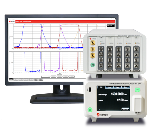
The STS – Swept Test System is engineered to characterize optical components with high accuracy and throughput. It measures wavelength-dependent loss (WDL), polarization-dependent loss (PDL), and insertion loss (IL) across a wide tuning range.
The STS is well-suited for analyzing filters, multiplexers, demultiplexers, and full PIC assemblies in co-packaged optics. The system uses a tunable laser source to sweep the desired wavelength range while capturing fine-grained optical responses. This is essential for validating the spectral performance of waveguides, ring resonators, or arrayed waveguide gratings embedded within a PIC.
With sub-dB accuracy and automated control, STS helps ensure component specifications are met before integration into CPO modules. It also supports multi-channel measurements, making it scalable for high-density applications.
To address the challenges of accurately aligning polarization, Santec has developed a combined solution using the TSL tunable laser, a polarization synthesizer, and the MPM power meter. This setup optimizes the input polarization state for effective coupling into the PIC waveguide. This approach offers higher measurement accuracy for insertion and polarization-dependent loss than standard polarization controllers. It also facilitates the characterization of components with high PDL values exceeding 30 dB, which cannot be reliably measured using conventional methods.
TSL-570 Type H – High Power Tunable Laser
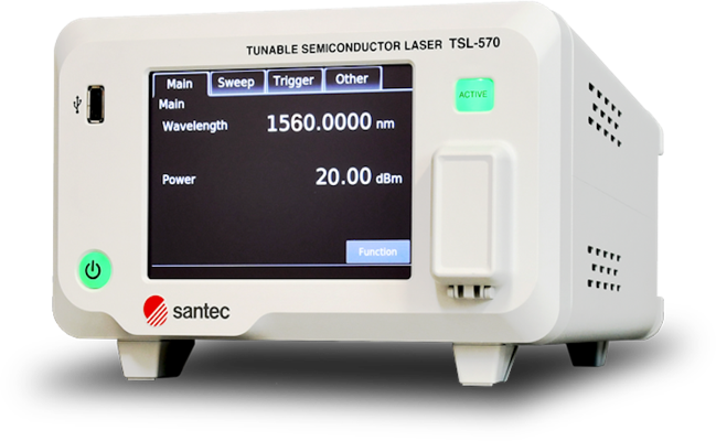
The TSL-570 Type H is a high-power tunable laser source that delivers optical output levels exceeding 20 dBm. This makes it ideal for high coupling loss, such as when aligning to edge-coupled or grating-coupled PICs inside co-packaged modules.
This laser enables clean and consistent signal injection across test setups. Its high resolution allows for fine wavelength scanning, while its output power compensates for the optical losses that occur during the testing of complex assemblies. This control and signal strength level ensures that measurements remain accurate for CPO systems with dense integration and limited test access points.
The TSL-570 Type H is also valuable in production environments, where fast and repeatable scans are required to validate each channel’s performance within a defined optical window.
TSL-570 Type H High Power Tunable Laser
PEM-400 – Polarization Extinction Ratio Meter
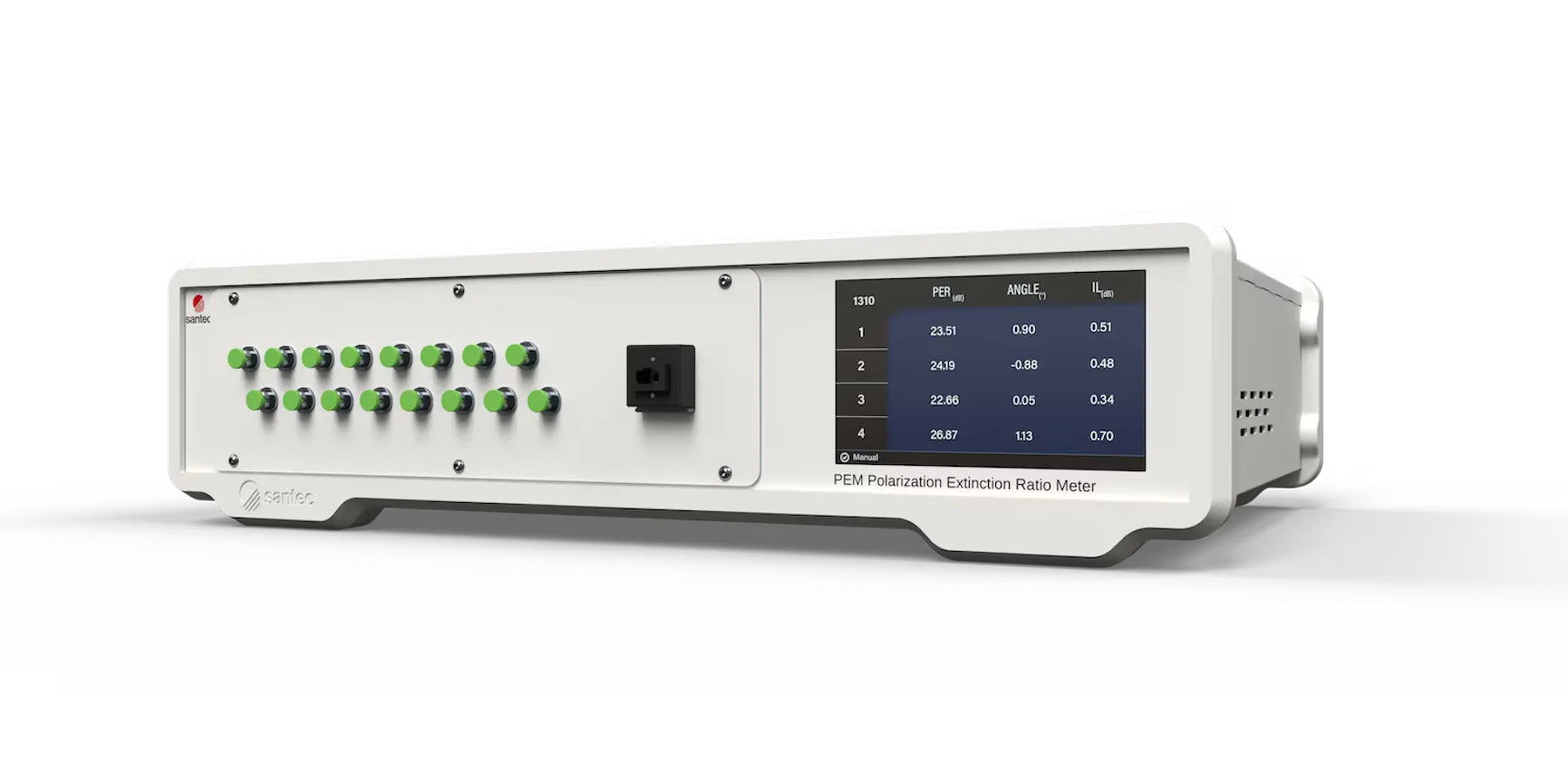
Polarization management is a known challenge in photonic integrated circuits. The PEM-400 addresses this by measuring the polarization extinction ratio (PER) of polarization-maintaining fibers and components used in CPO systems.
PER is an essential metric for determining how well a device maintains polarization state, especially in multi-channel systems. In CPO applications, where a mismatch in polarization alignment can lead to signal distortion or imbalance, accurate PER measurement helps prevent performance issues.
The PEM-400 supports multi-channel input, making it useful for testing fiber array units (FAUs) and other multi-port devices common in co-packaged designs. It also supports simultaneous insertion loss or output power measurement, streamlining validation, and shortening test cycles.
By providing reliable PER measurements, the PEM-400 ensures that polarization-sensitive PICs are properly aligned and performing within required thresholds.
PEM-400 – Polarization Extinction Ratio Meter
SPA-110 Swept Photonics Analyzer (Long Range Model)
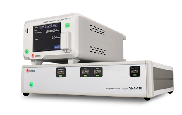
The SPA-110 uses Optical Frequency Domain Reflectometry (OFDR) to deliver high-resolution characterization of optical components, with a scanning range of up to 90 nm. It is designed for applications that demand precise reflectance, transmission, and loss analysis across photonic devices.
This system offers sub-6 µm spatial resolution, enabling the identification of localized features such as propagation loss, reflections, and structural discontinuities within compact photonic integrated circuits (PICs). Its performance is especially useful for evaluating components with fine geometries or closely spaced elements, as often found in co-packaged optics.
In CPO workflows, the SPA-110 supports both wafer-level and module-level inspection. It can detect issues like cross-talk, misalignment, or fabrication defects early in the process. Engineers can also use it to perform simultaneous insertion loss (IL), return loss (RL), and WDL measurements with high dynamic range and precision.
As system density increases, so does the importance of detailed spatial analysis. The SPA-110 provides the visibility required to ensure PIC quality before final integration, supporting development and high-volume production.
SPA-110 Swept Photonics Analyzer
Conclusion
Co-packaged optics are changing how data centers, AI clusters, and high-performance systems are built. Their ability to reduce power use, increase bandwidth, and maintain signal integrity makes them a key technology moving forward. As the margin for error becomes narrower, the need for precise and repeatable testing is unavoidable. Without it, yield and reliability are at risk.
Santec supports this shift with tools designed specifically for CPO validation. Their systems help engineers meet performance targets at every stage, from development to production. As CPO adoption grows, continued innovation in test equipment will be critical to support scalability and system performance.