
晶圆/芯片级测试
晶圆及芯片级测试是光子器件从设计概念迈向可制造产品的重要阶段。在这一阶段,测试工作的重点不仅在于获取光谱数据,更在于以满足工程开发效率的速度完成测试,并具备足够的分析能力,将器件真实特性与耦合、反射或光路连接等测试因素造成的影响区分开来。
Santec 通过以软件为核心的测试平台支持这一流程,结合扫频光谱表征、多端口测量、原位 OFDR 分析以及可扩展的光开关架构,为研发和生产环境提供灵活且高效的测试解决方案。
探索应用方案
晶圆/芯片级测试:封装前的工艺计量与性能验证
曾经有一位工艺工程师花费三周时间追查一个看似由分光器树状结构(Splitter Tree)引起的良率问题,最终却发现绝大部分性能差异并非来自器件本身,而是源于探针耦合过程的不稳定性。
那些在首次测试中表现不佳的裸片(Die),在重新调整光纤探针位置后再次测试时,性能均恢复正常。问题从未存在于晶圆之中,而是出现在测试流程本身——该流程无法区分耦合不稳定与器件真实性能之间的差异。
这种测试不确定性在晶圆级阶段所带来的成本,远高于后续生产阶段。
对于已经完成封装的器件,不合格产品可以直接淘汰;而在晶圆测试阶段,误判则会带来更严重的后果。假阴性(False Negative)可能导致性能不足的裸片进入后续封装流程,而假阳性(False Positive)则可能使本应合格的裸片被提前报废。
无论哪种情况,都会延缓测试、设计与制造之间的反馈循环。而在光子器件开发过程中,这一循环本身就已经是整个研发流程中最耗时且最具挑战性的环节之一。
一个真正有效的晶圆/芯片级测试方案需要同时满足三个目标:
* 以足够的精度完成光学性能表征,为工程决策提供可靠依据;
* 在测试环境内快速定位异常,而无需额外搭建分析流程;
* 能够适应不同裸片数量和端口配置,并在被测器件(DUT)变化时保持测试平台的可扩展性,而无需重新构建测试系统。
保留工程价值的光谱表征测试
晶圆级测试的基本要求,是能够对决定器件是否值得进入封装阶段的关键结构进行准确、可靠的光谱测量,包括:
* 波导(Waveguides)
* 分光器(Splitters)
* 光滤波器(Filters)
* 阵列波导光栅(AWGs)
* 环形谐振器件(Ring-Based Devices)
* 光路由结构(Routing Elements)
在晶圆级测试中,测试速度固然重要,但不能以牺牲测量分辨率为代价。
如果扫描速度足以满足高通量筛选需求,却因为采样过于粗略而遗漏通带内 30 pm 级别的波纹特征,那么这种测试并非更高效,而只是获得了更少有价值的信息。
这正是 TSL-570 的设计重点所在。
TSL-570 兼具最高 200 nm/s 的高速扫描能力、0.1 pm 波长分辨率以及在长时间连续运行条件下仍能保持稳定的波长精度,从而兼顾测试效率与测量质量。
对于希望提升测试吞吐量,同时保留完整工程分析价值的晶圆测试团队而言,真正值得关注的指标并非单纯的最高扫描速度,而是在高速测试条件下依然能够保持高分辨率和高精度测量能力。
光器件链路分析仪
该系统采用光频域反射技术(Optical Frequency Domain Reflectometry,OFDR),可对回波反射(Back Reflection)和传输特性(Transmission Characteristics)进行分析。凭借 5 μm 的空间采样分辨率,系统能够轻松识别光子集成电路(PIC)及硅光子(SiPh)器件内部的结构特征。
多端口采集的挑战在于测试效率,而不仅仅是硬件配置
许多晶圆级 PIC(光子集成电路)结构会产生多个输出端口,而在不断变化的测试条件下逐个端口进行串行测量,往往是导致测试数据难以准确解读的主要原因之一。
对于分光网络(Splitter Networks)、阵列波导光栅(AWGs)以及波长路由结构(Wavelength Routing Structures)等器件而言,需要测量的端口数量往往较多。此时面临的问题不仅仅是测试时间的增加,更重要的是不同端口测量过程中测试条件可能发生细微变化。
在这种情况下,串行测量得到的数据不仅反映器件本身特性,也同时受到系统漂移(Drift)的影响,从而降低数据的可比性和可信度。
MPM-220 正是针对这一挑战而设计。其支持:
* 最多 20 个端口同步采集(Simultaneous Multi-Port Acquisition)
* 每个端口最高 100 万个数据记录点
* 与 Santec 可调谐激光器配合使用时,实现实时参考插入损耗测量(Real-Time Referenced IL Measurement)
对于晶圆级测试而言,参考测量的稳定性与端口数量同样重要。
事实上,许多测试流程的效率瓶颈并不在于激光器扫描速度,而在于系统能否在所有输出端口测量期间持续保持一致且稳定的测试条件
当光谱测试无法提供答案时,需要原位故障分析能力
光谱异常能够说明某处存在问题,但无法直接告诉工程师问题出现在哪里。
在晶圆级测试环境中,这一区别具有重要意义。
例如:
* 谐振峰畸变(Resonance Distortion)
* 无法解释的插入损耗突变(Insertion Loss Step)
* 通带不对称(Passband Asymmetry)
这些现象可能来源于多种不同因素,包括:
* 器件本身的光子结构设计
* 局部波导缺陷(Localized Waveguide Defect)
* 光纤耦合误差(Coupling Artifact)
* 光传播路径中的不连续点(Propagation Discontinuity)
如果将这些问题统一归因于设计本身,并直接进入设计迭代阶段,往往会导致大量不必要的开发成本和时间投入。
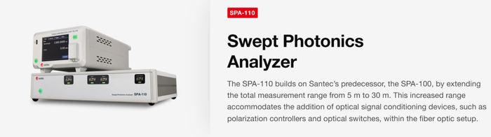
SPA-110 正是针对这一诊断需求开发的基于 OFDR(光频域反射技术)的分析平台,其主要特性包括:
* 5 μm 空间采样分辨率
* 最大 30 m 测量范围
* 最大 160 nm 扫描范围
* 同时实现光回波损耗(ORL)与波长相关损耗(WDL)表征
此外,系统还配备直通端口(Feedthrough Port),可连接外部光功率计,用于有源硅光器件(Active Silicon Photonics)的对准与测试。
在实际应用中,这意味着工程团队能够直接从异常光谱结果出发,快速定位具体问题位置并完成空间分辨分析,而无需更换测试平台或重新建立测试流程。
这种从“发现异常”到“定位根因”的连续测试能力,对于加速硅光研发、提高晶圆测试效率以及缩短设计迭代周期具有重要价值。
耦合稳定性:影响测试一致性的隐性因素
在晶圆级测试中,测试结果相关性(Correlation)不佳最容易被忽视的原因,往往并非仪器精度不足,而是信号进入仪器之前发生在光学接口处的问题。
探针与光栅耦合器(Grating Coupler)之间的对准漂移、光纤放置状态的不一致,以及不同测试之间参考条件的变化,都可能导致两个结构完全相同的裸片表现出截然不同的测试结果。
换句话说,看起来性能较差的器件,问题未必出在器件本身,而可能来自测试接口的不确定性。
这也是为什么 STS 系统的实时功率参考功能(Real-Time Power Referencing)以及 MPM-220 的光学参考端口(Optical Reference Port)不仅仅是规格参数,而是影响测试质量的重要工程设计。
SPA-110 在有源硅光器件对准过程中支持外部光功率计集成,同样遵循这一设计理念。
这三种方案背后的核心思想是一致的:在对器件性能做出判断之前,首先减少光学接口带来的不确定性。
无需重建测试平台即可实现扩展
如果一个晶圆测试平台在被测器件(DUT)从单一无源结构切换到复杂光路由器件时,或从研发调试阶段转向批量筛选阶段时,需要对测试系统进行大幅调整,那么这样的系统将成为开发流程中的负担,而非优势。
测试平台的可扩展性取决于以下几个关键因素:
* 光路切换架构(Routing Architecture)
* 光开关重复性(Switching Repeatability)
* 通道数量扩展能力
* 在系统扩展过程中保持既有测试逻辑和验证流程不变的能力
OSX-100 正是针对这一需求而设计的可扩展光开关平台,其主要特性包括:
* 支持从 1×2 到 1×400 的灵活配置
* ±0.005 dB 重复性
* 小于 0.5 dB 的插入损耗
* 低于 -80 dB 的串扰性能
同时支持 USB 和以太网(Ethernet)控制接口,可直接集成至自动化测试流程之中。
因此,当测试矩阵规模扩大时,无需为每次系统扩展重新启动独立的集成项目,从而降低测试平台升级和维护成本。
软件决定数据能否转化为工程决策
高速硬件本身并不能构建完整且高效的晶圆级测试流程。
如果缺少相应的软件平台支持,测试配置将变得复杂,测试方法难以保持一致,数据分析速度也无法满足工程开发需求。
一个有效的晶圆测试环境需要做到:
* 简化系统配置和测试流程建立
* 保证测试方案(Recipe)的一致性
* 快速完成数据处理和分析
* 在晶圆仍处于测试平台时即可输出可执行的工程结论
STS 平台配备专用软件系统,并支持基于 DLL 的自动化控制接口,涵盖:
* 系统配置管理
* 基础测试操作
* 数据分析
* 光回波损耗(ORL)测量
* 高分辨率光谱表征
等完整功能模块。
其设计目标并非简单地将多个仪器集中在同一个工作台上,而是构建一个统一的测试环境,使光源、检测、光路切换以及数据分析作为一个完整工作流程协同运行,从而帮助工程团队更高效地完成晶圆级测试与分析工作。


