
制造工艺监测
制造工艺监测只有在能够足够早地发现工艺漂移并及时调整生产过程时,才能真正创造价值,而不仅仅是在问题发生后记录失效结果。
Santec 的光学计量解决方案结合晶圆级映射、高速三维表面轮廓测量以及基于 OCT 的检测技术,帮助工程与生产团队持续监测工艺变化、分析根本原因,并将定量测量数据反馈至工艺控制系统,从而提升生产稳定性与产品良率。
探索应用方案
制造工艺监测:面向工艺控制的在线光学计量
在现代高精度制造过程中,无论是半导体晶圆、光子集成电路(PIC)还是先进微电子封装,质量管理的目标早已不仅仅局限于产线末端的缺陷筛查。
制造工艺监测需要在生产过程中尽早提供可重复、可量化的测量数据,为工艺调整和纠正措施提供依据。
其核心目标在于:
* 更早发现工艺漂移(Process Drift)
* 缩短工艺反馈周期(Feedback Loop)
* 减少不合格产品的持续累积
相比单纯发现问题,更重要的是在问题扩大之前识别并控制其发生。
无损检测内部结构与体积完整性
表面外观往往无法准确反映器件的实际功能性能。
对于多层结构、晶圆键合(Wafer Bonding)以及各类镀膜组件而言,许多工艺偏差往往发生在材料内部,而非表面。
因此,制造工艺监测系统不仅需要观察表面形貌,还需要具备以下能力:
* 测量层厚(Layer Thickness)
* 检测内部空洞(Sub-surface Voids)
* 识别分层缺陷(Delamination)
* 验证材料均匀性(Material Uniformity)
并且在整个过程中无需破坏样品。
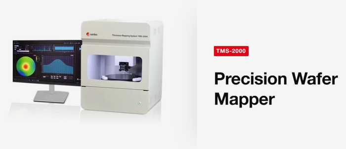
晶圆厚度测量系统
专为半导体与光电产业打造,提供自动化、非接触式、高速的晶圆厚度(Wafer Thickness)、总厚度变化(TTV)以及亚表面缺陷检测与成像功能。
由于扫频源光学相干断层扫描(SS-OCT)基于低相干干涉技术(Low-Coherence Interferometry),其轴向深度信息能够独立于横向扫描分辨率获取。
这一特性使其特别适用于:
* 光学半透明材料内部结构检测
* 键合界面质量评估
* 多层结构内部缺陷分析
* 在线实时无损检测
对于生产团队而言,其价值十分直接:能够在后续组装或封装工序增加成本之前发现内部缺陷,并获得可量化、可追溯的计量数据,而不仅仅依赖人工视觉判断。
满足生产节拍要求的高速尺寸计量
在自动化制造环境中,测量时间直接影响生产效率。
如果检测流程需要:
* 将样品移出生产线;
* 等待离线分析;
* 再将分析结果反馈至生产环节;
那么工艺调整将被延迟,不合格产品也可能持续产生。因此,要让制造工艺监测真正发挥作用,复杂的三维形貌数据和体积测量数据必须在生产节拍允许的时间范围内完成采集与分析。
实现这一目标的关键,很大程度上取决于系统所采用的光学引擎(Optical Engine),尤其是激光光源的扫频速度。
以 HSL 系列高速扫频光源为代表的高速扫频架构,可提供满足高速检测需求的波长扫描性能,并支持高达数十万次 A-Scan/秒的测量速率。
借助这种高速扫描能力,系统能够在较大测量区域内实现高密度、高分辨率的三维测量,同时避免计量环节成为生产流程中的效率瓶颈。
对于需要在线检测(Inline Inspection)和实时工艺控制(Process Control)的先进制造环境而言,高速测量能力已不仅仅是性能优势,更是实现规模化生产监测的基础条件。
缺陷定位与定量形貌分析
当制造工艺开始出现漂移时,单纯的合格/不合格(Pass/Fail)结果通常不足以支持有效的工艺调整。
工程师需要获得与具体物理位置相关联的尺寸和形貌信息,例如:
* 镀膜均匀性偏差(Coating Non-uniformity)
* 晶圆边缘微裂纹(Wafer-Edge Micro-cracks)
* 沟槽深度偏差(Trench Depth Deviation)
* 台阶高度误差(Step Height Error)
* 表面粗糙度变化(Surface Roughness Variation)
* 上游设备加工造成的局部损伤(Localized Tool-Induced Damage)
如果缺乏这些具体信息,即使发现了异常,也很难将计量结果与实际工艺参数调整建立直接关联。
因此,一个有效的工艺监测系统不仅需要发现问题,更需要同时具备:
* 缺陷定位能力(Defect Localization)
* 定量测量能力(Quantitative Measurement)
高精度光学轮廓仪(Optical Profiler)可提供包括表面粗糙度、台阶高度以及沟槽深度在内的定量表面形貌数据;而体积成像技术则能够提供具有空间位置信息的亚表面结构数据。
两类技术结合后,可在三维空间内对缺陷和尺寸偏差进行精确映射,并实现微米级甚至亚微米级灵敏度检测。
对于工艺工程师而言,这些数据不仅能够发现异常,更能够帮助追溯问题根因,将失效现象与具体设备状态、工艺参数变化或生产条件联系起来,从而支持更加精准的工艺优化。
面向生产环境的测量稳定性
能够在研发实验室中获得优异性能的光学测量系统,并不一定能够在实际生产环境中保持同样表现。
在制造现场,测量系统通常需要面对多种环境因素的影响,包括:
* 机械振动(Vibration)
* 温度波动(Temperature Fluctuation)
* 有限安装空间(Constrained Installation Space)
* 不同设备之间的相互干扰(Machine-to-Machine Interaction)
这些因素都会直接影响测量结果的稳定性和重复性。
因此,用于工艺监测的光学计量设备必须从设计阶段就考虑生产环境需求,而不能依赖实验室条件下的隔振平台或严格环境控制。
这也是模块化系统架构(Modular System Architecture)具有重要价值的原因。
通过将坚固耐用的光学扫描头(Ruggedized Optical Scan Head)与对环境更敏感的光源及数据处理模块分离设计,可以将测量单元直接集成到:
* 自动化机器人工作单元(Robotic Cells)
* 在线卷材检测系统(Web Inspection Lines)
* 自动化生产设备
等工业环境中,同时保持亚微米级测量所需的干涉测量稳定性。
在实际工厂部署过程中,决定系统可用性的因素不仅仅是标称分辨率(Nominal Resolution)。
更关键的指标包括:
* 长时间运行稳定性(Long-Term Stability)
* 环境干扰容忍能力(Environmental Robustness)
* 连续生产过程中的性能一致性(Continuous Operation Performance)
只有同时满足这些要求,光学计量系统才能真正成为生产过程控制的一部分,而不仅仅是一套实验室测量工具。
数据处理与决策支持层
高速干涉测量系统能够产生海量数据。
然而,仅有原始干涉信号(Interferograms)或未经处理的三维点云数据(3D Point Clouds),并不能帮助生产团队更快地做出决策。
只有当测量系统能够将复杂数据转换为可理解、可比较且可执行的工艺参数时,制造工艺监测才能真正发挥价值。
因此,软件层在整个工艺监测体系中扮演着至关重要的角色。
一个有效的数据处理平台需要具备以下能力:
* 实时数据渲染(Real-Time Visualization)
* 自动特征提取(Automated Feature Extraction)
* 尺寸分析(Dimensional Analysis)
* 自动化合格/不合格判定(Pass/Fail Evaluation)
从而帮助工程团队快速识别异常并采取相应措施。
结合高速数据采集卡(High-Speed Digitizers)与针对具体应用开发的数据处理软件,系统可实时执行快速傅里叶变换(Fast Fourier Transform,FFT)以及自动化尺寸分析,将关键测量参数直接计算并输出。
这些结果可进一步自动导出至工厂数据库或制造执行系统(MES),实现生产数据的统一管理与共享。
对于生产环境而言,这种自动化数据处理能力带来的价值主要体现在:
* 建立完整的数据追溯体系(Traceability)
* 支持长期趋势分析(Trend Analysis)
* 实现统计过程控制(Statistical Process Control,SPC)
* 提升工艺优化效率
* 减少人工数据分析负担
最终,工艺监测系统的价值并不在于生成更多数据,而在于帮助生产团队更快、更准确地完成决策。
通过将测量、分析与决策支持整合至统一平台,工程师能够及时发现工艺变化趋势,并在问题影响产品质量之前采取相应措施,从而提升生产稳定性和良率控制能力。


