
量子计算
量子计算对光学控制提出了极高要求。在量子门保真度、系统重复性以及从概念验证向大规模系统扩展的过程中,激光器性能发挥着关键作用。
本页面重点介绍量子计算应用中激光光源的实际仪器需求,包括波长可调谐能力、频率稳定技术(用于抑制噪声和频率漂移)以及光束调节技术,以实现对光强、频率和脉冲宽度的精确控制。
探索应用方案
量子计算:将光学控制视为系统稳定性问题
在量子计算领域,真正的挑战并不在于成功实现一次高保真量子门操作,而是在长时间实验过程中、跨多个量子比特(Qubits)以及大量连续运算下,持续保持相同的性能水平。
从工程角度来看,这本质上是一个系统稳定性问题。
无论量子比特采用何种物理实现方式,例如:
* 囚禁离子(Trapped Ions)
* 中性原子(Neutral Atoms)
* 超导电路(Superconducting Circuits)
* 金刚石氮空位中心(NV Centres)
* 半导体量子点(Semiconductor Quantum Dots)
决定系统性能的核心原则都是一致的。
系统必须在足够长的时间内,将频率(Frequency)、相位(Phase)、光强(Intensity)以及时序(Timing)控制在严格容差范围内,才能保证实验结果具有可信度和可重复性。
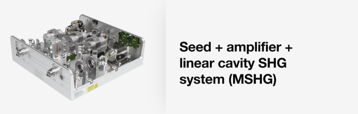
种子源 + 放大器 + 线性谐振腔倍频(SHG)系统
常见波长包括:用于镱(Ytterbium)的 798/399 nm,用于铷(Rubidium)的 840/420 nm 和 960/480 nm,用于锶(Strontium)的 922/461 nm,以及用于铯(Caesium)的 1020/510 nm。
对于中功率放大系统(0.5 至 5 W),整体倍频效率通常为 50% 至 60%;对于低功率直接外腔半导体激光器(ECDL)(例如 100 mW),则可通过优化实现更高的倍频效率(最高可达 70%)。
这种需求使量子计算的关注重点从“控制单个量子比特”逐渐转变为“为多个量子比特和多次量子操作维持稳定且可控的光学环境”。
虽然量子门保真度(Gate Fidelity)和量子门速度(Gate Speed)最终决定了量子处理器的整体性能,但实际限制系统性能的因素通常来自光学控制系统本身,包括:
* 频率稳定性(Frequency Stability)
* 相位稳定性(Phase Stability)
* 光强控制精度(Intensity Control Accuracy)
* 时序精度(Timing Precision)
* 空间模式质量(Spatial Mode Quality)
* 噪声水平(Noise Performance)
如果这些参数无法得到充分控制,误差将在连续操作过程中快速累积,使系统难以从实验室中的概念验证(Proof of Concept)扩展为具备实际应用价值的量子计算平台。
因此,一个面向量子计算的光学控制架构需要同时具备以下三项核心能力:
### 稳定的频率与相位参考
确保激光频率和相位在长时间运行过程中保持稳定,减少漂移和噪声对量子态操控的影响,为高保真量子门操作提供可靠基础。
### 精确且可重复的光强调制
能够对光功率进行高精度控制,并在重复实验中保持一致性,以确保每次量子操作获得相同的激励条件。
### 确定性的光脉冲生成
按照预定义的时序和相位关系生成光脉冲,实现对量子态演化过程的精确控制,并满足复杂量子算法和多量子比特操作对同步性的要求。
下面的内容将进一步讨论这些需求如何映射到实际系统架构,包括:
* 激光光源系统(Laser System)
* 频率稳定化层(Stabilization Layer)
* 光束调理与控制系统(Beamline Conditioning)
并重点结合囚禁离子量子计算(Trapped-Ion Quantum Computing)的典型应用场景,探讨高性能光学控制系统在量子计算中的关键作用。
光谱纯度与频率稳定性决定相位误差预算
在量子计算系统中,光场直接决定量子比特的相位演化过程。
由于激光频率噪声会直接映射为相位噪声,因此会限制量子相干时间(Coherence)并降低量子门保真度(Gate Fidelity)。这一影响在长时间量子门操作以及多量子比特控制过程中尤为显著,因为相位误差会随着时间持续累积。
激光器的本征线宽(Intrinsic Laser Linewidth)决定了系统能够达到的相位稳定性下限,而这一限制无法通过后续系统补偿完全消除。
对于半导体激光器而言,较高的线宽增强因子(Linewidth Enhancement Factor)会导致振幅噪声(Amplitude Noise)转换为频率噪声(Frequency Noise),进一步加剧相位不稳定性。
这一问题在蓝光和近紫外波段的直接发射氮化镓(GaN)激光二极管中尤为明显,因此往往成为限制系统性能的重要因素之一。
对于需要极低相位噪声的应用场景,采用窄线宽红外激光器并通过倍频产生目标波长,通常能够获得更稳定的性能表现(如 Santec MSHG 和 MSL 系列方案)。
虽然倍频过程会使线宽随光学频率增加而相应变化,但其整体性能通常仍优于直接发射方案。
因此,在量子计算系统中,光源架构的选择并非简单的实施细节,而是决定系统性能上限的重要设计决策。
频率漂移必须被持续抑制,而不是定期校正
除了激光线宽之外,长期频率漂移(Long-Term Frequency Drift)同样会影响量子计算系统性能。
频率漂移会导致失谐误差(Detuning Error),从而改变量子门操作过程中的相位关系和耦合强度,并随着时间推移降低系统重复性和实验一致性。
在这种应用场景下,仅依赖定期重新校准(Periodic Recalibration)的测量模式并不足以满足需求。
量子计算对于频率精度的要求通常需要持续的频率稳定化控制,并将激光频率实时锁定至稳定参考标准。
具体采用何种稳定化方案,取决于激光光源本身的噪声特性。
对于窄线宽激光器,可通过原子参考系统(例如 Santec MGSA)或高分辨率波长计(如 Santec FZW)实现频率稳定化,从而满足许多量子门操作所需的长期稳定性要求。
而对于线宽较宽或频率噪声较高的光源,则通常需要采用高带宽锁频系统,将激光器锁定至高稳定性光学腔体,以同时抑制短期频率噪声和长期频率漂移(如 Santec FSC 系列方案)。
无论采用哪种实现方式,频率稳定化都不应被视为附加功能。
对于量子计算系统而言,它属于关键的系统级设计环节,并直接决定系统是否能够达到目标精度和预期量子门保真度。
换言之,稳定化系统不仅影响性能优化,更决定整个量子控制架构能否满足实际应用需求。
光强稳定性决定作用点上的量子门精度
在基于拉曼跃迁(Raman-Based)实现的量子门操作中,激光光强直接决定拉比频率(Rabi Frequency),进而影响量子比特旋转的速度和精度。
因此,任何光强波动都会直接导致:
* 旋转过度(Over-Rotation)
* 旋转不足(Under-Rotation)
等控制误差,并随着量子门序列的执行不断累积,最终降低整体量子门保真度。
然而,影响量子门精度的因素并不仅仅是激光器输出端的相对强度噪声(Relative Intensity Noise,RIN)。
在实际系统中,以下因素同样会导致量子比特所接收到的有效光强发生变化:
* 光束指向稳定性(Beam Pointing Stability)
* 空间模式变化(Spatial Mode Variation)
* 光路中的机械漂移(Mechanical Drift)
从量子比特的角度来看,这些因素与激光器本身的强度噪声没有本质区别,因为它们都会表现为作用光强的变化。
因此,一个有效的量子光学控制系统不应仅仅稳定激光器输出功率,而应确保在实际作用于量子比特的位置实现光强稳定化(详见 Application Note AN001)。
这意味着系统不仅需要具备低本征噪声(Low Intrinsic Noise)的激光光源,还需要拥有能够长期保持空间模式和光束指向稳定性的光束传输架构(Beam Delivery System)。
换句话说,真正影响量子门精度的并不是激光器输出了多少光功率,而是量子比特实际接收到的光功率是否保持稳定。
脉冲生成与相位控制决定可用光波形质量
量子门操作通常依赖于严格定义的光脉冲序列实现。
这些光脉冲不仅需要精确控制时间位置,还必须保持明确且稳定的:
* 振幅(Amplitude)
* 频率(Frequency)
* 相位关系(Phase Relationship)
为了实现高保真量子控制,系统通常需要在纳秒至微秒时间尺度上完成波形生成和调制,同时保持:
* 极低时序抖动(Low Timing Jitter)
* 稳定的光学相干性(Phase Coherence)
这种级别的控制能力通常无法通过直接调制激光光源实现。
在实际量子计算系统中,更常见的方案是采用声光调制器(Acousto-Optic Modulator,AOM),并结合高性能射频电子系统进行驱动,从而实现对下游光信号的高速精密控制(如 Santec XRF 和 QRF 系列)。
这种架构能够提供:
* 高速光功率调制
* 精确频率偏移控制(Frequency Offset Control)
* 高精度脉冲时序控制
* 多路独立频率输出
* 更低的相对强度噪声(RIN)
* 面向容错量子计算的高速量子门控制能力
在该架构中,激光器的作用是提供稳定的光学载波(Optical Carrier),而真正决定光波形结构的则是后端的光束调理与控制层(Beamline Conditioning Layer)。
因此,量子门操作的重复性、执行速度以及最终保真度,很大程度上取决于这一控制层的性能表现。
如果说激光器决定了系统能够达到的性能上限,那么光束调理与波形控制系统则决定了这些性能能否被稳定、准确地转化为实际量子门操作。
换句话说,高性能量子计算所需要的并不仅是稳定的激光光源,而是一套能够持续产生可重复、可预测光波形的完整光学控制架构。
量子门保真度是一个多参数协同控制问题
量子门保真度(Gate Fidelity)并非由单一参数决定,而是受到多个关键控制变量共同影响。
频率噪声(Frequency Noise)、频率漂移(Frequency Drift)、光强波动(Intensity Fluctuation)以及时序误差(Timing Error)都会对量子门操作产生影响,并最终反映在系统整体保真度上。
因此,仅优化其中某一个参数,并不一定能够提升整体系统性能。
例如,即使采用超窄线宽激光器,如果光强调制不稳定或脉冲时序存在误差,量子门保真度仍然会受到明显限制。
换句话说,量子计算系统的性能通常由当前最薄弱的控制环节决定,而非由表现最好的单项指标决定。
为了实现高保真量子控制,所有关键参数都必须同时保持在预定容差范围内。
随着量子比特数量增加以及量子门序列不断延长,这些容差要求还会进一步收紧。
因此,从实验室原型验证发展到大规模量子处理器的过程中,系统设计的重点往往不再是提升单一性能指标,而是在多个控制维度之间维持长期、稳定且可重复的平衡。
光束调理层决定光学控制的实际可用性
实现上述控制要求的核心环节,通常位于光束调理层(Beamline Conditioning Layer)。
在这一层中,声光调制器(AOM)、射频信号源(RF Sources)以及反馈控制电子系统(Feedback Electronics)共同作用,将激光器所提供的光学稳定性转化为实际可执行的量子操作。
其主要功能包括:
* 主动光强稳定化(Active Intensity Stabilization),用于抑制振幅噪声(Amplitude Noise)
* 频率偏移控制(Frequency Shifting),用于定义拉曼失谐量(Raman Detuning)
* 高精度脉冲生成(Precise Pulse Generation),用于量子门时序控制
通过这些控制机制,系统能够将稳定的光学载波转换为满足量子计算需求的可编程光学波形。
随着量子门速度不断提高以及误差预算持续缩小,光束调理层的重要性已经逐渐接近激光光源本身。
即使两套系统采用相同规格的激光器,其最终量子门保真度仍可能存在显著差异,而差异往往来自于光束调理与控制架构的设计方式。
从工程角度来看,高性能量子计算并非仅依赖优质激光器,而是依赖完整的光学控制链路。
激光器负责提供稳定光源,稳定化系统负责维持频率与相位参考,而光束调理层则负责将这些稳定性转化为实际可执行且可重复的量子操作。
因此,光束调理层不仅是连接光源与量子比特之间的接口,更是决定系统最终控制精度和量子门保真度的关键环节。
实现规模化需要持续的系统级控制
在高度受控的概念验证(Proof-of-Concept)实验中,通过人工调节和定期重新校准,往往可以实现较高的量子门保真度。
然而,这种方式并不具备规模化应用能力。
随着量子比特数量增加、量子门序列变长以及系统运行时间延长,依赖人工干预的控制模式将变得越来越难以维持。
面向实际应用的量子计算系统需要的是持续、自动化且可重复的控制机制,并能够在长时间运行过程中保持稳定性能。
因此,系统设计的重点也随之发生变化。
挑战不再仅仅是选择性能更好的单个器件,而是如何构建一个能够长期协同运行的整体控制架构。
在这一架构中,激光光源、频率稳定化系统、光束传输系统以及射频控制平台必须作为统一系统共同工作,而非彼此独立的功能模块。
只有当这些子系统之间形成稳定且可预测的协同关系时,量子计算平台才能在保持高保真度的同时实现进一步扩展。
光学控制决定量子计算性能能否实现规模化
高保真囚禁离子量子门的性能并不仅仅取决于量子比特本身的物理特性。
更重要的是,控制系统是否能够在长时间运行过程中持续维持稳定且可预测的光学环境。
频率、相位、光强以及时序等关键参数都必须被控制在严格的容差范围内,确保误差累积速度始终低于系统纠错和补偿能力。
如果无法实现这种持续控制,即使单次实验能够获得优异结果,也难以支撑更复杂、更长时间的量子运算任务。
从这个角度来看,激光系统并非量子处理器之外的辅助设备。
它本身就是量子计算架构的重要组成部分。
激光系统的设计架构和性能水平,直接决定了系统能够达到的量子门保真度、实验重复性以及未来可扩展性。
因此,对于先进量子计算平台而言,光学控制系统不仅承担信号生成和传输功能,更构成了整个量子处理器稳定运行的基础。
随着量子计算向更高量子比特数量、更复杂算法以及更长运行时间发展,系统级光学控制能力将成为决定平台性能上限的重要因素之一。


