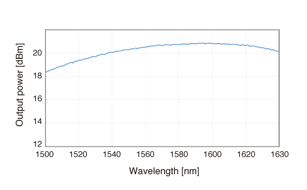
高い出力パワー
20 dBm を超える光出力パワー

TSL-570 Type Hは、20 dBm を超える光出力パワーを備えた高性能、高出力モデル波長可変レーザです。
高度な光学キャビティ設計により、ピコメートルの精度、サブピコメートルの解像度、および最大 200 nm/秒の高速スキャンが可能です。 TSL-570 Type H は、O-band(1260~1360nm)、または、CL-band(1500~1630nm)に対応しています。サンテックの波長可変レーザは、光学部品の特性評価、光集積回路評価、量子フォトニクス、分光法、センサーなど、フォトニクス分野で広く使用されています。特にTSL-570 Type Hは、高出力の波長可変レーザーとして材料損失や結合損失が大きい光デバイスを高密度に集積したシリコンフォトニクスの検証・評価に最適です。
20 dBm を超える光出力パワー
環境温度変化に対して、優れた設定波長安定性を実現しています。
高い分解能を維持したまま、最大200 nm/sの速度で波長掃引が可能です。
0.1 pm の波長分解能と精度を提供します。
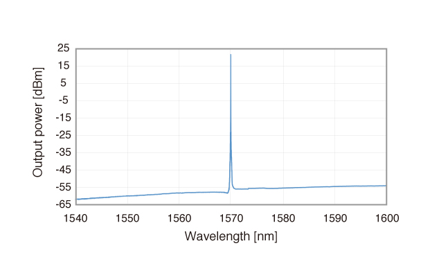
自然放出光レベルを低く抑え、信号に対する自然放出光(SNR)は 90 dB/0.1 nm を実現しています。
最小 10 GHzの微調整が可能です。
Silicon photonics has become a foundational technology in high-speed data communication, integrated photonic circuits (PICs), and next-generation optical systems. This comprehensive whitepaper delivers an in-depth, engineer-friendly introduction to silicon photonics — exploring its physical principles, key device architectures, and measurement challenges.
In this whitepaper, you will discover:
1. The fundamentals of silicon photonics: waveguides, modulators, and photodetectors
2. Common silicon photonic device designs (e.g., ring resonators, Mach-Zehnder modulators)
3. Key performance metrics, such as insertion loss, extinction ratio, and modulation bandwidth
4. Measurement techniques and best practices for silicon photonic component testing
5. How tunable lasers, stable wavelength sources, and precision power meters can be integrated into a silicon photonics test setup
6. Practical system design tips to improve measurement accuracy and yield
This guide also explains how Santec’s tunable lasers, wavelength stabilization solutions (Laser Lock Pro), and high-performance optical power meters can support your silicon photonic device development and qualification workflow.
Read the full whitepaper
Co-packaged optics (CPO) is revolutionizing data center and high-performance computing interconnects by integrating optical engines directly with switching ASICs. This whitepaper offers a detailed, engineer-level exploration of CPO, covering both the technological benefits and the rigorous testing requirements needed to ensure performance and reliability.
In this whitepaper, you will discover:
1. The key drivers for CPO adoption — power efficiency, bandwidth scaling, signal integrity, and form-factor optimization
2. How photonic integrated circuits (PICs) enable compact, high-density optical I/O in CPO architectures
3. Thermal challenges in co-packaged designs and best practices for thermal management during testing
4. Testing strategies for CPO modules: measuring insertion loss, return loss, polarization effects, crosstalk, and more
5. Advanced measurement solutions: how Santec’s tunable lasers, polarization synthesizers, power meters, and swept analyzers (e.g., STS system, SPA-110) can be integrated into high-precision CPO validation setups
6. Practical tips for building an automated, repeatable test flow that addresses the unique trade-offs of co-packaged optics
Whether you're developing PICs for production, characterizing module-level performance, or optimizing test processes for yield and scale, this guide shows how Santec’s measurement instruments support every aspect of CPO development.
Read the full whitepaper


