
光部品特性評価
コンポーネント試験では、「十分」とされる測定が見えない歩留まり低下につながることがあります。santecのコンポーネント試験ソリューションは、広帯域にわたる高速かつ再現性の高いスイープ特性評価(WDL/PDL)を実現。リアルタイムリファレンスと量産対応の自動化により、フィルタ、DWDM/AWGデバイス、WSSモジュール、カプラ、スプリッタなどを高い信頼性で評価できます。光学特性に異常値がある場合でも、高速3D検査を追加することで、ラインを止めることなくパッケージや光学系の形状・表面品質を検証できます。
アプリケーションソリューション
なぜコンポーネント検査・試験には「単一測定」ではなく「システム」が必要なのか
受入検査を終えたフィルタチップを用いて作成されたDWDMの生産ラインにおいて、不具合が多発する事象が発生しました。調査の結果、その原因は製品不良ではなく、合格判定に用いられた測定条件にありました。受入検査の測定条件が50pmステップだったため、パスバンド内に存在していた80pmのリップルを捉えられなかったことが判明しました。一見、問題ないように見えた光スペクトルでも、光部品としては不適合となります。この種の問題は、想像以上に頻発しており、その原因の多くは「光部品の特性を評価する」のではなく「数値を得る」ことを目的に設計された測定ワークフローに起因します。
近年の受動素子や多チャンネル光部品は、顕在化しにくい形で不具合を生じる可能性があります。たとえば、十分なサンプリング設定で初めて現れるスペクトルリップル、特定の偏波状態で現れるPDLペナルティ、特定のポート組み合わせでのみ発生する後方反射などです。こうした現象を確実に捉えるためには、単一的な測定とその合否判定に頼るのではなく、多角的なシステムレベルで設計された測定ワークフローが不可欠です。
測定を始める前に「何を測っているのか」を定義する
測定を開始する前に、まず「何を測定しているのか」を明確に定義することが不可欠です。特に実験室において「光部品間のばらつき」と見なされている現象の多くは、実際にはデバイス固有の特性ではありません。その要因の一つが、基準面(reference plane)が適切に定義されていないことによるものです。
測定器の選定や試験手順を作成する前に、以下の3つのポイントを明確にする
- 評価指標: 単一波長での挿入損失(IL)か、帯域平均ILか、パスバンドリップルか、PDLか、チャネル間均一性か
- 基準面: コネクタ端面なのか、ピグテール端なのか、あるいはアダプタを含むのか
- 測定条件: 入射状態、コネクタの装着状態、温度、接続間の待機時間など
このステップを省略すると、同じデバイスを測定している2人のエンジニアが異なる結果を出すことになり、どちらも間違いではないという状況が生じます。測定自体は正しくても、「何を測っているか」の定義が存在していないのです。この曖昧さは、大量生産や複数拠点におけるサプライヤ認定において、致命的な問題に発展する要因となります。
光学特性検査システム
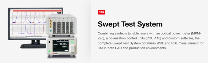
Santecの波長可変レーザー、光パワーメータ、偏波制御ユニット、専用ソフトウェアを統合し、研究開発および生産環境向けにWDL・PDL測定を最適化します。
ドリフトは校正の問題ではなく、測定系設計の問題
波長掃引における挿入損失(IL)測定は、光部品とは無関係なゆっくりとした変動の影響を受けやすい特性があります。例えば、長時間のスイープ中に生じる光源出力のドリフトや、リファレンス測定と本測定の間で発生するコネクタの微小なずれ、さらには温度変化によるファイバの複屈折の変動などです。多くの研究室では、これらを頻繁な再校正で対応すべき問題と捉えていますが、それは適切なアプローチではありません。
重要なのは、測定プロセスそのものにリアルタイムのパワーリファレンスを組み込み、ドリフトを断続的に補正するのではなく連続的に打ち消すことです。スイープ中にリアルタイムでパワー補正するシステムは、意図した通りの光部品測定を可能にします。一方で、その機能がないシステムは、光部品に加え、前回の校正以降に生じたあらゆる変動を含めて測定することになります。特に量産環境では、その校正間隔は長すぎます。このため、専用のリファレンスポートや補正チャネルを備えたスイープ測定アーキテクチャは、たとえ波長可変レーザや検出器の仕様が類似していても、本質的に異なる測定性能を示します。
偏波依存損失(PDL)は、挿入損失(IL)測定では見えなかった最悪条件の挙動を明らかにする
単一の偏波状態でILが良好に見える光部品でも、偏波を全域で掃引すると全く異なる特性が現れる場合があります。アイソレータ、薄膜フィルタ、そして光路に異方性を持つ構造を含むデバイスは、標準的なIL測定では仕様を満たしているように見えても、PDLによって実運用時にシステムペナルティを引き起こすことがあります。
多くのコヒーレント系や高密度WDM環境ではPDLの影響は無視できません。そのため、試験ワークフローでは以下を明確に規定する必要があります。
- 偏波状態をどのように生成するのか
- どれだけの偏波状態をサンプリングするのか、あるいは連続的な偏波スクランブルを用いるのか
- 測定データ群からどのように代表値を算出し測定結果とするのか
ミューラーマトリクス掃引に基づく最大値と最小値の差 (Max–Min) と、ランダムスクランブルに対する統計的エンベロープは同等ではなく、得られる仕様マージンも一致しません。どの手法を採用するかは製品ごとに決定し、明文化するべきであり、ロットごとに再検討するものではありません。
スペクトルサンプリングは、問題が発生するまで規定されないパラメータ
同一の光部品を2つの測定ステーションで評価し、異なる挿入損失(IL)の結果が出た場合、その原因の多くは他の要因に先立ち「サンプリング設定」にあります。100pmのステップサイズは一般的ですが、これは測定が高速でトレースもきれいに見える一方で、重要な特性を見逃してしまいます。たとえば、パスバンド端に存在する狭帯域ノッチ、コネクタ内のエタロン効果による周期的リップル、25pm以下でなければ分解できないチャネル不均一性などです。
対策はシンプルですが、確実な運用が求められます。サンプリング設定、ステップ間隔、掃引速度、平均化条件を測定仕様として明文化し、それを単なる調整パラメータではなく「試験の一部」として扱うことです。これにより、測定ステーション間の差異は追跡可能なものになります。これがなければ、そもそも本質的に異なる測定結果を比較していることになります。
マルチポートデバイスでは、「数多くの測定」ではなく「比較可能な測定」が求められる
アレイ導波路回折格子(AWG)、波長選択スイッチ(WSS)、カプラ、マルチチャネルスプリッタにおいて重要なのは、多数のポートにアクセスできることではありません。重要なのは、それらのポート間の測定結果が、実際の製造判断に使えるレベルで相互に比較可能であることです。チャネル間のばらつきを評価する際、各チャネルの測定不確かさが検出したいばらつきと同程度であれば、その測定データは意味を持ちません。
これを実現するには、真に同時のマルチポート測定、あるいはポート間の再現性が十分に特性化され、安定しており、その影響が仕様マージンに織り込まれているスイッチングアーキテクチャが必要です。特に有効なのが「リファレンスポート」の考え方です。これは、全チャネルの測定中に1つのポートを継続的に監視し、補正基準として用いる手法であり、スイッチングベースの構成において測定間の比較性を維持する上で非常に効果的です。これに相当する仕組みがなければ、ロット間の判定は本来考慮されていない測定ノイズを含んだものとなり、判断精度を損なう結果につながります。
後方反射スクリーニングは、不具合解析ではなく標準フローに組み込む
リターンロス(RL)への感度が高まっているシステムにおいて、後方反射の問題は往々にして別の現象として現れます。例えば、動作の不安定性、パスバンドリップルのように見える挙動、予期しないゲイン変動などです。反射が最初から疑われることは少なく、原因として特定される頃には、他の要因の追及に多くの時間が費やされてしまいます。
より実用的なアプローチは、IL評価と並行して高速な反射スクリーニングを標準工程として組み込むことです。これは、受入検査や組立前試験の段階で実施することが有効です。特にマルチチャネルデバイスでは、ポートごとのリターンロスのばらつきは、挿入損失のばらつきと同等に重要な指標となります。また、両者を同時に測定しても、片方のみを測定する場合と比べて追加される時間はごくわずかです。
光学測定データで説明できない場合は、パッケージに着目する
明確な光学トレースが得られたからといって、アセンブリが正しく構成されているとは限りません。パッケージ化されたコンポーネントには、より大きな問題として顕在化するまで光学トレース上には直接現れない不具合モードが存在します。例えば、レンズのスタンドオフ誤差による作動距離のずれ、接合位置のオフセットによる温度変化に伴った徐々な結合ずれ、さらにはARコーティングの表面状態に起因し特定の入射角でのみ現れる後方反射などが挙げられます。
光部品の特性が継続的に規格外であり、光学的な再測定でも原因が特定できない場合、最短の解決策は再度の光学スイープではなく、パッケージ形状そのものを直接測定することです。パッケージレベルでの高速3D表面プロファイリングを用いれば、非破壊で数分以内に実装状態が設計通りであるかを確認できます。研究開発では試作と評価の反復サイクルを短縮し、量産では原因不明の不良品をトレーサブルな根本原因へと変える手段となります。


