Optical Power Measurement for High-Volume Photonics Test
Introduction
Optical power measurement is a dependency for most photonics test workflows, including component characterization, subsystem integration, and production screening. In high-volume environments, the dominant failure modes are rarely “meter broken.” They are typically workflow-level: unstable reference conditions, wavelength/polarization mismatch, connector contamination, drift between reference and test states, or untracked setup changes.
When power measurement is used to compute insertion loss, gain, or pass/fail thresholds, small systematic biases can shift yield classification and process capability metrics. The practical requirement is not only a calibrated optical power meter, but a measurement chain that is stable, repeatable, and auditable across operators, stations, and time.
This paper focuses on: (1) what the instrument reports, (2) how detector physics drives error terms, (3) calibration meaning and limits, and (4) test-setup controls that scale to manufacturing use cases, including automated logging and periodic verification.
What Is Being Measured
Optical Power vs Optical Energy
Optical power is the rate of energy transfer (W). Optical energy is the time integral of power (J). Many fiber optic test applications use continuous wave (CW) or quasi-CW signals where power is the controlled and reported quantity.
For modulated signals, an optical power meter reports average power over its integration time. Peak power, modulation depth, and waveform features require separate measurement methods.
Units Engineers Actually Use: W, dBm, dB
W / mW / µW: Absolute power in physical units.
dBm: Absolute power expressed on a logarithmic scale referenced to 1 mW.
- P(dBm)=10log10(P(mW))
- P(mW)=10P(dBm)10
dB: A ratio between two power levels (relative measurement). dB is not an absolute unit.
Insertion loss and gain are typically computed in dB.
A common workflow error is mixing dBm (absolute) and dB (relative) without explicitly defining the reference state and measurement plane.
Crucial Unit Distinction: dBm vs. dB
Remember: dBm is absolute power (referenced to 1 mW), while dB is a relative ratio (gain or loss). A common production error is mixing these units without defining the measurement plane—ensure your automated scripts explicitly track the reference state.
Multi-Port Optical Power Meter

Why insertion loss variation is the first yield problem to control
Insertion loss and optical power are central manufacturing metrics because they directly affect link budgets and system margin. At wafer level, however, absolute IL is measured through a coupling condition that differs from the final package. The manufacturing value of IL is therefore determined by consistency and correlation, not by absolute optical loss alone.
Uncontrolled coupling variation turns IL into a mixed metric. It contains device loss, grating or edge coupling state, source power drift, detector response, polarization state, and environmental disturbance. When those terms move together, a stable device population can look unstable.
|
Problem signal |
What goes wrong physically |
Measurement architecture response |
|
IL shifts across sites or retests |
FAU working gap, lateral alignment, angular alignment, polarization state, and reference power are changing with the test cell. |
Use stable reference monitoring, simultaneous or tightly synchronized power acquisition, and alignment routines that optimize repeatability rather than only peak coupling. |
How stable does a wafer-level PIC test need to be?
Repeatability requirements are defined by process capability and decision margin. A measurement that is repeatable on a bench can fail in production once integrated with a wafer prober, automated motion, continuous optical sweeping, and long operating hours.
At scale, stability emerges from the combined behavior of optical measurement, mechanical positioning, thermal equilibrium, and sequencing logic. Treating these contributors independently underestimates the uncertainty that reaches the pass/fail decision.
How to Build a Silicon Photonics Wafer Test Uncertainty Budget
How to mitigate thermal drift in automated silicon photonics probing
Thermal drift changes the geometry between the FAU and the wafer. Lateral alignment, angular alignment, and standoff distance all shift as the stage, fixtures, coupling head, and surrounding structures move toward a new thermal equilibrium. The optical response is often nonlinear because coupling efficiency changes rapidly near alignment thresholds.
In production, thermal equilibrium is rarely static. Continuous stage motion, repeated probing sequences, optical/electrical loading, and nearby electronics create localized thermal patterns that evolve during the wafer map. Measurements taken at different times or locations can therefore include thermal artifacts that resemble process drift.
- Monitor common-mode drift through reference paths or reference structures.
- Separate source/detector drift from coupling drift whenever possible.
- Use measurement sequences that avoid reinforcing localized thermal gradients.
- Treat warm-up and settling as production parameters, not laboratory conveniences.
|
Problem signal |
What goes wrong physically |
Measurement architecture response |
|
Slow IL trend across wafer, lot, or shift |
Thermal expansion changes FAU pose/gap and the optical reference state over time. |
Reference-channel monitoring, stable swept-source operation, multi-port power logging, and deterministic sequence timing help distinguish instrument drift from coupling drift. |
The "Layered Control" Strategy for HVM
Don't rely solely on annual calibration. Implement a three-tier defense:
(1) Formal traceable calibration,
(2) Interim verification using transfer standards, and
(3) Station-level logging for early drift detection.
High-Performance Tunable Laser

How to reduce mechanical misalignment and grating coupler alignment error
Mechanical misalignment directly affects wafer-level optical coupling. In non-contact optical probing, the relevant variables are not contact force but lateral position, angular alignment, working gap, scan repeatability, and FAU flatness relative to the wafer surface. For grating coupler alignment, a small Z or angular error can move the measurement outside the intended coupling condition.
The problem becomes harder when several ports must be aligned at once. A single-channel optimum may not be the array optimum, and a mechanically acceptable position for one port may place another port close to a coupling slope. The uncertainty budget must therefore account for port-to-port alignment gradients, not only global alignment error.
- Use automated optical alignment routines when manual or static alignment cannot maintain repeatability.
- Track coupling statistics per port, not only total transmitted power.
- Evaluate alignment repeatability over wafer maps and shifts, not only during setup.
|
Problem signal |
What goes wrong physically |
Measurement architecture response |
|
Retest variation after apparently successful alignment |
Alignment optimized peak coupling at setup but did not control array-level pose/gap repeatability during automated operation. |
Automated optical alignment, FAU-aware scan routines, and per-channel power acquisition help detect array gradients before they become yield errors. |
How to control vibration and environmental coupling at the wafer interface
Factory vibration differs from laboratory vibration. Floor motion, adjacent equipment, wafer handlers, acoustic coupling, and motion stages can modulate the optical interface during acquisition. Sub-micron motion can become visible in insertion loss, particularly with dense fiber arrays and short integration windows.
Environmental coupling is intermittent and load-dependent. It may not appear during a short acceptance test but can emerge when the tool is placed near production equipment or when the motion sequence changes.
- Measure during settled mechanical states unless synchronized acquisition is intentionally used.
- Avoid interpreting vibration-induced variance as device non-uniformity.
- Verify integration time against the actual disturbance spectrum of the installed tool.
|
Problem signal |
What goes wrong physically |
Measurement architecture response |
|
Noise increases only during production operation |
Mechanical vibration overlaps acquisition time and modulates coupling before the detector integrates. |
Coordinate motion control and optical acquisition deterministically; use integration windows and settling times based on the installed environment. |
Why multi-port PIC probing errors do not add linearly
In a simple uncertainty budget, independent contributors can be approximated by root-sum-square addition. Multi-port wafer-level optical testing rarely satisfies that condition. Thermal drift, FAU misalignment, source variation, polarization changes, and optical crosstalk often affect several ports at the same time, creating correlated errors.
As port count increases, a small common-mode shift can move many measurements together. That is why a component-level specification can look acceptable while the full test cell produces unstable manufacturing decisions.
- Separate common-mode drift from per-port variation.
- Prefer simultaneous or tightly synchronized multi-channel acquisition when port-to-port correlation matters.
- Use reference channels to identify source and path drift before attributing trends to the wafer.
|
Problem signal |
What goes wrong physically |
Measurement architecture response |
|
RSS uncertainty looks acceptable but pass/fail variation remains high |
Errors are partially correlated across ports due to shared optical, mechanical, or thermal states. |
Multi-port optical power acquisition, reference monitoring, and channel-level logging help identify correlated uncertainty before it becomes false yield loss. |
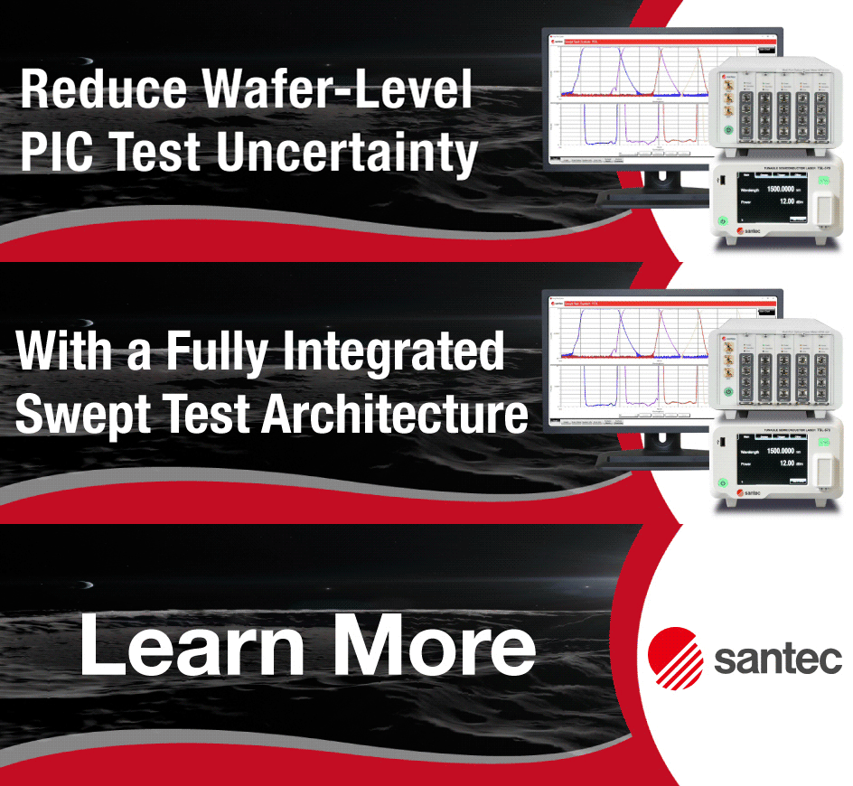
Swept Test System
One platform. All critical measurements.
Built for high-volume silicon photonics manufacturing.
How Many Optical Ports Can Be Tested in Parallel Before Uncertainty Wins?
How optical crosstalk affects multi-channel FAU probing
Optical crosstalk becomes a limiting mechanism as more ports are measured simultaneously. It can arise from proximity effects in fiber arrays, shared optical paths, imperfect isolation, reflections, and leakage between adjacent waveguides or fibers. In manufacturing, this produces correlated port errors rather than isolated channel noise.
Crosstalk matters most near decision boundaries. A small leakage term can distort insertion loss or optical power enough to change a borderline pass/fail decision, especially when adjacent channels have significantly different power levels.
Why thermal and optical coupling increase with port count
Parallel testing increases the density of optical paths, electronics, fixtures, and acquisition channels. Heat from nearby electronics or optical dissipation can create channel-dependent drift across an array. At the same time, lateral or angular error across the FAU can appear as a systematic power gradient.
Beyond a certain port count, adding channels no longer reduces total test time proportionally. The added verification, alignment recovery, and uncertainty management can dominate the expected throughput gain.
Mechanical limits of FAU and silicon photonics wafer prober design
The mechanical limit of a high-port-count wafer-level test is set by array pitch, head stiffness, flatness, stage repeatability, and the ability to maintain stable working gap across all active channels. Software can compensate for some repeatable offsets, but it cannot eliminate physical gradients that change during operation.
- Large arrays require array-level alignment, not only center-channel alignment.
- FAU flatness and angular repeatability become direct uncertainty contributors.
- Calibration cannot fully remove drift that changes between calibration and measurement.
Why parallelization is not only a throughput strategy
In wafer-level PIC manufacturing, parallelization is often dictated by the DUT. Many devices expose multiple co-dependent optical ports that must be measured in one test instance to understand the device state. Throughput improvement is a useful consequence, but it is not always the primary reason for multi-port testing.
The practical question is therefore not “how many ports can the instrument support?” It is “how many ports can be measured before correlated uncertainty, recovery time, and alignment verification degrade the manufacturing decision?”
When More Ports Mean Less Throughput
Throughput in PIC testing is constrained by an inflection point. Beyond a critical port count, the overhead for setup, alignment verification, and error handling outweighs the speed gains of simultaneous measurement, leading to diminishing returns.
Multi-Port Optical Power Meter
Eliminate uncertainty from port-to-port variation with synchronized, high-speed acquisition.

How Fast Can You Test Before Measurement Validity Breaks?
How integration time changes precision and false yield loss
Integration time controls the trade-off between speed and measurement precision. Short integrations increase throughput but raise susceptibility to detector noise, transient coupling changes, vibration, and source drift. Long integrations improve precision but reduce capacity and can average over changing states.
The correct integration time is therefore process-dependent. It must be selected against decision margin, coupling stability, environmental disturbance, and required confidence, not only against instrument noise floor.
How alignment tolerance affects test cycle time
Alignment routines consume a large portion of wafer-level test time. Tight alignment targets improve coupling but can increase search time, convergence time, and verification time. In production, the goal is repeatable alignment within the decision margin, not necessarily the absolute maximum optical power at every site.
Overly aggressive alignment can reduce net throughput without improving yield confidence. Under-aggressive alignment produces unstable IL and optical power data. The useful operating point lies between those extremes.
How to map manufacturing tolerance to measurement speed
Manufacturing tolerances define the allowed measurement uncertainty for pass/fail decisions. Measurement speed must be chosen so combined uncertainty remains below that tolerance with enough margin to cover drift and environmental variation.
- Start from allowable pass/fail uncertainty, not from maximum instrument speed.
- Include coupling repeatability, source stability, detector stability, synchronization, and calibration drift.
- Validate the selected speed under production-like duty cycle.
How to identify accuracy breakpoints under production constraints
Accuracy breakpoints occur when a small increase in speed causes a disproportionate loss of measurement validity. The breakpoint may come from insufficient settling, shorter integration, unstable alignment convergence, thermal drift, or timing mismatch between motion and acquisition.
A sustainable test sequence operates below the breakpoint. Operating beyond it can temporarily improve apparent throughput while degrading long-term yield stability and increasing retest burden.
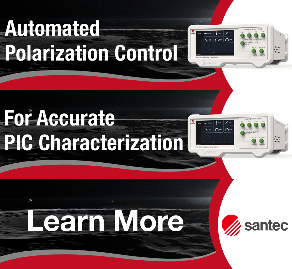
Polarization Control Unit
Designed for polarization-sensitive devices, PDL measurements, and automated swept-wavelength testing.
How to Improve Wafer-to-Package Correlation
Why wafer-level and packaged-device data diverge
Correlation between wafer-level and packaged-device measurements is critical for screening. Divergence arises because wafer probing and packaged testing use different coupling conditions, thermal environments, mechanical constraints, and sometimes different polarization states.
Weak correlation does not always mean wafer data are useless. It often means the wafer test system is adding uncontrolled variation that hides the relationship between wafer metrics and packaged performance.
How coupling efficiency variation creates screening errors
Coupling efficiency changes substantially between wafer probing and packaged interfaces. A die that appears marginal at wafer level may perform acceptably after packaging, while a die that passes wafer screening may fail later if the wafer test did not capture the relevant mode or polarization condition.
Thresholds must therefore be set with knowledge of coupling-state variation and its correlation to downstream performance, not as direct translations of packaged insertion loss limits.
How statistical methods improve wafer-to-package prediction
Regression, correlation analysis, and multivariate classification can improve wafer-to-package prediction when the wafer-level measurement is stable. These methods combine several wafer metrics into a decision model and can reveal trends that single thresholds miss.
Their weakness is sensitivity to measurement drift. If the wafer data set contains uncontrolled coupling or calibration variation, statistical models learn the test system as much as the device population.
How weak correlation creates hidden yield loss
Weak correlation creates hidden yield loss through false rejects and false accepts. The cost becomes visible downstream, after packaging or system integration, when corrective action is more expensive. Increasing wafer-test speed does not solve this problem if the underlying correlation remains weak.
What Optical Instruments Must Survive in Production Mode
6.1 How continuous operation changes measurement stability
Optical instruments behave differently under continuous production duty cycle than during short laboratory checks. Thermal loading, component aging, wavelength sweep repetition, optical path changes, and environmental exposure can produce drift only after hours of operation.
Production validation must therefore include long-run behavior. A short benchmark can confirm capability but cannot prove shift-level stability.
How to manage calibration drift under high-throughput conditions
Calibration drift introduces systematic bias across large data sets. In high-throughput operation, recalibration opportunities are limited, so drift monitoring must be built into the measurement strategy rather than treated as occasional maintenance.
- Use reference signals to detect source and path drift.
- Track detector response and optical path state over time.
- Define recalibration intervals from production evidence, not calendar habit alone.
Why warm-up and settling time belong in the test recipe
Warm-up and settling behavior affects repeatability after power cycling, configuration changes, wafer transitions, or maintenance events. Early measurements after a change may differ from steady-state measurements, producing artificial shifts in wafer data.
A production test recipe should specify when the instrument and optical path are considered settled. Otherwise, transient behavior becomes an uncontrolled uncertainty source.
How Automation Sequencing Creates or Reduces Test Variability
How motion control settling affects optical measurement repeatability
Motion control defines where the optical interface is when acquisition begins. If residual motion remains after a move, the measurement captures a transient coupling state rather than the intended settled state. This increases variance even when the optical instruments are stable.
How test sequencing changes thermal and mechanical stability
Sequence order affects thermal load distribution and mechanical settling. Repeated move-measure cycles can accumulate local heat, while scan patterns that revisit adjacent sites can reinforce drift. A move, settle, measure sequence behaves differently from overlapped motion and acquisition.
- Use deterministic sequencing for production recipes.
- Validate scan order against thermal drift and retest statistics.
- Avoid changing sequence order without rechecking uncertainty and correlation.
Why optical and mechanical subsystems must be synchronized
Synchronization errors create measurements taken during the wrong mechanical or optical state. As throughput increases, the margin between motion completion, source state, detector acquisition, and software logging shrinks. Deterministic coordination is essential for repeatability.
How to Maintain FAU Coupling Repeatability Under Factory Conditions
How fiber array coupling repeatability affects wafer-level PIC probing
FAU coupling repeatability depends on stable non-contact coupling to the wafer. Variability in standoff distance, lateral position, and angular alignment directly changes measured insertion loss and optical power. This is why grating coupler alignment and edge-coupling setup must be treated as manufacturing variables, not setup details.
How mechanical and thermal coupling mechanisms shift the optical interface
Differential expansion and structural compliance create coupled mechanical and thermal behavior. The same tool can behave differently across shifts, wafer lots, or facility locations if environmental conditions and operating history change.
How alignment drift accumulates over test cycles
In non-contact optical probing, alignment drift accumulates through gradual mechanical settling, fixture creep, thermal variation, and changing interface cleanliness, rather than through deliberate physical contact. Small changes in standoff or angular alignment shift measurement baselines over time.
|
Problem signal |
What goes wrong physically |
Measurement architecture response |
|
Baseline shifts over repeated wafer maps |
The FAU-to-wafer coupling state is changing while the test recipe assumes it is fixed. |
Use periodic alignment verification, reference structures, coupling statistics, and controlled cleaning/inspection intervals. |
Swept Photonics Analyzer
Analyze reflectance, transmission, propagation loss, and wavelength-dependent loss with OFDR technology.

How Test Uncertainty Causes False Fail and False Pass Decisions
How measurement uncertainty contributes to yield loss
Measurement uncertainty causes yield loss when it approaches the manufacturing tolerance. A die near the pass/fail threshold can change classification because of test-system variation rather than device performance. Across large volumes, small uncertainty growth becomes visible as false yield loss.
How to set guard bands without hiding process capability
Guard bands reduce false passes by tightening acceptance criteria, but they increase false fails. Excessive guard banding can hide the true process capability by converting test instability into apparent process weakness.
- Guard bands should be based on measured system-level uncertainty.
- They should be reviewed when the test recipe, tool, FAU, source, detector, or sequence changes.
- They should account for correlated multi-port behavior, not only independent noise terms.
Balancing Yield Risk and Quality
Optimal guard bands must be defined by system-level variability. While they mitigate the risk of false passes, excessive guard-banding can lead to significant yield loss by triggering frequent false fails.
How to quantify false fail and false pass risk
False fails reduce usable yield; false passes propagate marginal devices downstream. Quantifying both requires stable test behavior and realistic uncertainty estimates. Without this, manufacturing decisions rely on assumptions rather than evidence.
Practical Boundaries for Scalable Wafer-Level PIC Testing
How to find the maximum reliable parallelization level
The maximum reliable level of parallelization is defined by system stability, not theoretical channel count. Beyond the reliable boundary, crosstalk, correlated drift, alignment recovery, and retest burden offset the benefit of simultaneous measurement.
How stability requirements impose speed limits
Stability requirements impose upper bounds on useful test speed. Sustainable speed is more valuable than peak speed because it preserves decision confidence across shifts and lots.
A trade-off framework for throughput versus measurement validity
A scalable wafer-level PIC test strategy should define throughput using the complete system: measurement uncertainty, alignment repeatability, thermal behavior, calibration state, port count, and pass/fail tolerance.
- Define the decision margin first.
- Measure system-level uncertainty under production-like duty cycle.
- Identify speed and port-count breakpoints experimentally.
- Select the operating point below the breakpoint, not at the theoretical maximum.
- Revalidate after hardware, software, sequence, or FAU changes.
Instrumentation Functions That Map to These Failure Modes
The goal is not to promote a single instrument as a universal answer. The correct architecture depends on the DUT, port count, coupling method, wavelength band, polarization sensitivity, and production constraints. However, the measurement functions below directly address the failure modes described in this paper.
Failure mode |
Required function |
Typical instrument class |
Santec implementation reference |
Wavelength-dependent loss or PDL variation during sweeps |
Coordinated swept source, power acquisition, polarization handling, and software sequencing |
Swept photonics test system |
STS Swept Test System: tunable laser + MPM-220 + PCU + software |
Multi-port IL and optical power instability |
Synchronized multi-channel power acquisition and reference monitoring |
Multi-port optical power meter |
MPM-220 Multi-Port Optical Power Meter |
Polarization-dependent measurement ambiguity |
Controlled polarization state or Mueller Matrix style PDL measurement |
Polarization control unit |
PCU-200 Polarization Control Unit |
Unexplained reflections, path discontinuities, or localized loss |
Spatially resolved reflectance/transmission/path analysis |
OFDR swept photonics analyzer |
SPA-110 Swept Photonics Analyzer |
Use this table as an engineering mapping layer. The technical requirement is always the same: choose instrumentation that reduces or isolates the uncertainty source before it reaches the manufacturing decision.